
In Part 1 of this power-system optimization series, we examined how power-supply noise sensitivity can be quantified and how these quantities can be connected to real effects in the signal chain. The question was asked: What are the real noise limits to achieve superior performance of high-performance analog-signal-processing devices? Noise is just one measurable parameter in designing a power distribution network (PDN).
As noted in Part 1, a pure focus on minimizing noise can come at the cost of increased size, higher cost, or lower efficiency. Optimizing a PDN improves these parameters, while lowering noise to necessary levels.
This article builds on the generalized overview of the effects of power-supply ripple in high-performance signal chains. Here, we dive deeper into the details of optimizing PDNs for high-speed data converters. We compare a standard PDN to an optimized PDN to see where gains can be made in space, time, and cost. Upcoming Part 3 will explore specific optimization solutions for other signal chain devices, such as RF transceivers.
In This Content
Power-System Optimization for the AD9175 DAC
The AD9175 is a dual, 16-bit digital-to-analog converter (DAC) that supports DAC sample rates up to 12.6 GS/S. The device features an 8-lane,15.4-Gb/s JESD204B data input port; a high-performance, on-chip DAC clock multiplier; and digital-signal-processing capabilities targeted at single-band and multiband direct-to-radio-frequency (RF) wireless applications.
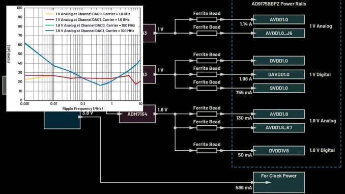
Let’s look at optimizing a PDN for this dual high-speed DAC. Figure 1 shows the standard power distribution network for the AD9175 as installed on the off-the-shelf evaluation board. The PDN comprises an ADP5054 discrete quad switcher and three low-dropout (LDO) post regulators. The goal is to see if this PDN can be improved and simplified, while ensuring its output noise doesn’t cause any significant degradation in performance.
The AD9175 requires eight power rails, which can be collected into four groups:
- 1-V analog (two rails)
- 1-V digital (three rails)
- 1.8-V analog (two rails)
- 1.8-V digital (one rail)
Analysis: Noise Requirements
Before we can optimize anything, we must understand the power-supply sensitivity of these rails. We will focus on the analog rails, as they tend to be more sensitive to noise than the digital rails.
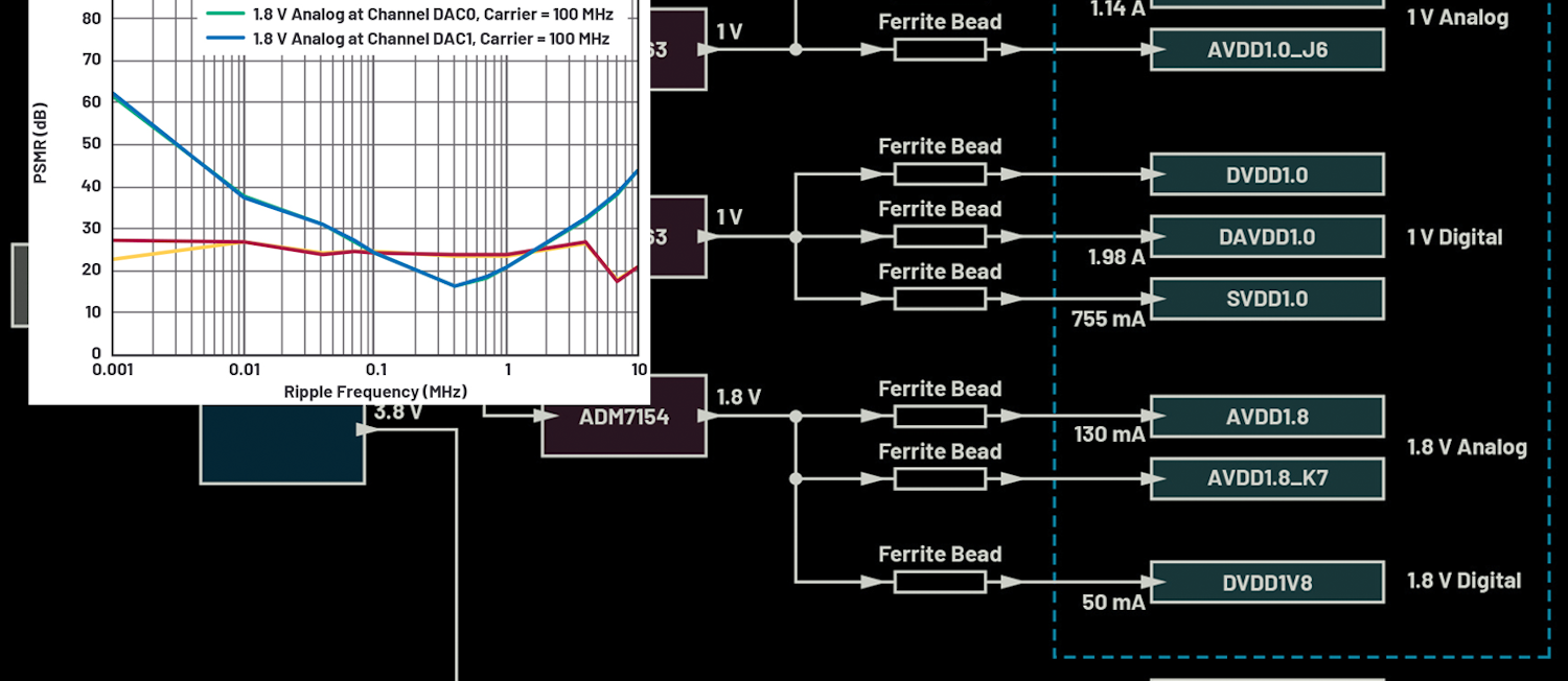
Figure 2 shows the power-supply modulation ratio (PSMR) of the analog rails. Note that the 1-V analog rails are relatively more sensitive at the 1/f frequency region, while the 1.8-V analog rails are more sensitive in the range of switching-converter operating frequencies (100 kHz to around 1 MHz).

One approach to optimization is to use a low-noise switching regulator with an LC filter. Figure 3 shows the conducted spectral output of the LT8650S Silent Switcherregulator (with and without an LC filter) with spread-spectrum frequency modulation (SSFM) mode off.
As discussed in Part 1, SSFM reduces the switching-frequency noise amplitude but introduces noise peaks in the 1/f region due to the triangular modulation frequency. This added noise would exceed the maximum allowable ripple threshold for this rail as the 1/f noise already has a small margin from that threshold. Thus, SSFM isn’t recommended to be used in this case. The maximum allowable voltage ripple threshold represents the power-supply ripple level at which when exceeded, sideband spurs in the DAC carrier signal appear above the 1-µV p-p noise floor of the DAC output spectrum.
It can be seen from these results that the 1/f noise of the switching regulator doesn’t exceed the maximum allowable ripple threshold of the 1-V analog rail. Also, an LC filter is sufficient to knock down the fundamental switching ripple and harmonics of LT8650S below the maximum allowable ripple threshold.
Figure 4 shows the conducted spectral output of the LT8653S (with and without an LC filter). Also shown is the maximum allowable voltage ripple for the 1.8-V rail that will not produce spurs in the 1-µV p-p noise floor of the AD9175 output spectrum. As can be seen, the 1/f noise of the LT8653S doesn’t exceed the maximum allowable ripple threshold, and an LC filter is sufficient to knock down the fundamental switching ripple and harmonics of LT8653S below the maximum allowable ripple threshold.
Results: Optimized PDN
Figure 5 illustrates an optimized power distribution network of the AD9175. The goal is to raise efficiency and reduce space requirements and power loss over the PDN in Figure 1 while achieving AD9175 superior dynamic performance. The noise goals are based on the maximum allowable ripple threshold shown in Figures 3 and 4.
The optimized PDN consists of LT8650S and LT8653S Silent Switcher regulators followed by LC filters on the analog power rails. In this PDN, the 1-V analog rail is powered by the VOUT1 of the LT8650S followed by an LC filter; the 1-V digital rail is directly powered by the VOUT2 of the same LT8650S, no LC filter required. For the AD9175, the digital rails are less sensitive to power-supply noise, so directly powering these rails is possible without degrading the DAC dynamic performance. The LT8653S with LC filter directly powers the 1.8-V analog and 1.8-V digital rails.
Table 1 compares the performance of the optimized PDN to the standard PDN shown in Figure 1—a quad buck switcher with three LDO regulators. The component area reduction of the optimized solution is 70.2% over the standard. Furthermore, efficiency is increased to 83.4% (from 69.2%) with an overall power saving of 1.0 W.

To verify that the noise performance of the optimized PDN is sufficient to meet high-performance specifications, the AD9175 is evaluated in terms of phase noise and inspecting the DAC output spectrum of sideband spurs around the carrier.1 Phase-noise results are within datasheet specification limits (Table 2). The output spectrum of AD9175 has a clean carrier frequency with no visible sideband spurs (Fig. 6).

 using the optimized PDN.")
Power-System Optimization for the AD9213 ADC
The AD9213 is a single, 12-bit, 6-GS/s or 10.25-GS/s, RF analog-to-digital converter (ADC) with a 6.5-GHz input bandwidth. The AD9213 supports high dynamic-range frequency and time-domain applications requiring wide instantaneous bandwidth and low conversion error rates (CERs). The AD9213 features a 16-lane JESD204B interface to support maximum bandwidth capability.
Figure 7 shows a standard power distribution network for the AD9213—as found on the off-the-shelf evaluation board—consisting of an LTM4644-1 µModule quad switcher and two linear regulators. This solution is fairly space- and energy-efficient, but can it be improved?

As noted in this series, the first step to optimization is quantifying the sensitivity of AD9213—that is, realistically setting the limits of PDN output noise so that it doesn’t significantly degrade the ADC’s performance. Here we’ll look at an alternate PDN solution using two µModule regulators and compare its performance against the standard off-the-shelf solution.
The AD9213 10 GSPS ADC requires 15 different power rails, collected into four groups:
- 1-V analog (three rails)
- 1-V digital (six rails)
- 2-V analog (two rails)
- 2-V digital (four rails)
Analysis: Noise Requirements
The optimized solution we’re exploring replaces an LTM4644-1 µModule quad switcher and two linear regulators with two µModule regulators, the LTM8024 and the LTM8074, and a single LDO post regulator.
Figure 8 shows the PSMR results for 1-V and 2-V analog power rails of the AD9213 at a 2.6-GHz carrier frequency. The 1-V analog rail is more sensitive than the 2-V analog rail due to a lower PSMR.

Figure 9 presents the spectral output of the LTM8024 (with and without an LDO regulator) in forced continuous mode (FCM). Also shown is an overlay of the maximum allowable voltage ripple threshold that will not produce spur in the –98-dBFS noise floor of the AD9213 output spectrum. The unfiltered 1/f noise and fundamental switching spur of LTM8024 output exceed the maximum allowable ripple threshold when directly powering the 1-V analog rail.

Adding an ADP1764 LDO post regulator to the LTM8024 reduces the 1/f noise and fundamental switching ripple and its harmonics down to the maximum allowable ripple threshold (Fig. 9, again). Some overhead voltage is required at the input of the linear regulator. In this case, a 1.3-V output is used from the LTM8024 to the input of the post regulator. This 300 mV meets the recommended headroom voltage specification of the LDO regulator while minimizing power loss in it—this is slightly better than the 500 mV in the standard solution.
Addressing the 2-V rails: Figure 10 illustrates the spectral output of the LTM8074 µModule regulator (with and without an LC filter) in FCM. The maximum allowable voltage ripple threshold also is shown. This threshold represents the power-supply ripple level at which when exceeded, sideband spurs in the ADC carrier signal appear above the –98-dBFS noise floor of the AD9213 output spectrum. Here, similar to the 1-V analog rail, the regulator switching spurs exceed the maximum allowable ripple threshold when directly powering the 2-V analog rail. An LDO regulator isn’t required, though. Instead, an LC filter at the LTM8074 output reduces the switching spur below the maximum allowable ripple threshold.

Results: Optimized PDN
Figure 11 depicts the optimized PDN resulting from the power-supply sensitivity evaluation results. Like the standard solution, it uses three power ICs: an LTM8024, LTM8074, and ADP1764. In this solution, the LTM8024 µModule regulator VOUT1 is post-regulated by the ADP1764 to power the relatively sensitive 1-V analog rail. The 1-V digital rail is directly powered by VOUT2 of LTM8024. Much like the AD9175 DAC, the AD9213’s digital rails are less sensitive to power-supply noise, so directly powering these rails is possible without degrading the ADC dynamic performance. The LTM8074 with LC filter powers the 2-V analog and 2-V digital rails.

Table 3 compares the performance of the optimized PDN to the standard off-the-shelf PDN. As shown in Figure 7, the standard PDN uses a quad buck switcher with two LDO regulators. Component area reduction is 15.4% and efficiency increased to 73.5% (from 63.1%) with an overall power saving of 1.0 W.
To verify the performance of the optimized PDN, the AD9213 is evaluated in terms of SFDR and SNR, and by inspecting the FFT output spectrum of the sideband spurs around the carrier. The SNR and SFDR performance show results that are within datasheet specifications limits (Table 4). Figure 12 shows the FFT output spectrum of AD9213; it features a clean carrier frequency with no visible sideband spurs.
